As of late 2025, the semiconductor industry has reached a pivotal turning point with the official commencement of high-volume manufacturing (HVM) for Intel’s 18A process node. This milestone represents the successful completion of the company’s ambitious "five nodes in four years" roadmap, a journey that has redefined the company’s internal culture and corporate structure. With the 18A node now churning out silicon for major partners, Intel Corp (NASDAQ: INTC) is attempting to reclaim the manufacturing leadership it lost nearly a decade ago, positioning itself as the primary Western alternative to the long-standing advanced logic duopoly of TSMC (NYSE: TSM) and Samsung Electronics (KRX: 005930).
The arrival of 18A is more than just a technical achievement; it is the centerpiece of a high-stakes corporate transformation. Following the retirement of Pat Gelsinger in late 2024 and the appointment of semiconductor veteran Lip-Bu Tan as CEO in early 2025, Intel has pivoted toward a "service-first" foundry model. By restructuring Intel Foundry into an independent subsidiary with its own operating board and financial reporting, the company is making an aggressive play to win the trust of fabless giants who have historically viewed Intel as a competitor rather than a partner.
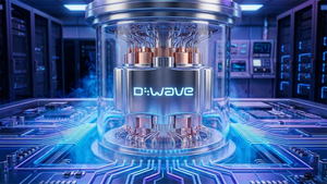
The Technical Edge: RibbonFET and the PowerVia Revolution
The Intel 18A node introduces two foundational architectural shifts that represent the most significant change to transistor design since the introduction of FinFET in 2011. The first is RibbonFET, Intel’s implementation of Gate-All-Around (GAA) technology. By replacing the vertical "fins" of previous generations with stacked horizontal nanoribbons, the gate now surrounds the channel on all four sides. This provides superior electrostatic control, allowing for higher performance at lower voltages and significantly reducing power leakage—a critical requirement for the massive power demands of modern AI data centers.
However, the true "secret sauce" of 18A is PowerVia, an industry-first Backside Power Delivery Network (BSPDN). While traditional chips route power and data signals through a complex web of wiring on the front of the wafer, PowerVia moves the power delivery to the back. This separation eliminates the "voltage droop" and signal interference that plague traditional designs. Initial data from late 2025 suggests that PowerVia provides a 10% reduction in IR (voltage) droop and up to a 15% improvement in performance-per-watt. Crucially, Intel has managed to implement this technology nearly two years ahead of TSMC’s scheduled rollout of backside power in its A16 node, giving Intel a temporary but significant architectural window of superiority.
The reaction from the semiconductor research community has been one of "cautious validation." While experts acknowledge Intel’s technical lead in power delivery, the focus has shifted entirely to yields. Reports from mid-2025 indicated that Intel struggled with early defect rates, but by December, the company reported "predictable monthly improvements" toward the 70% yield threshold required for high-margin profitability. Industry analysts note that while TSMC’s N2 node remains denser in terms of raw transistor count, Intel’s PowerVia offers thermal and power efficiency gains that are specifically optimized for the "thermal wall" challenges of next-generation AI accelerators.
Reshaping the AI Supply Chain: The Microsoft and AWS Wins
The business implications of 18A are already manifesting in major customer wins that challenge the dominance of Asian foundries. Microsoft (NASDAQ: MSFT) has emerged as a cornerstone customer, utilizing the 18A node for its Maia 2 AI accelerators. This partnership is a major endorsement of Intel’s ability to handle complex, large-die AI silicon. Similarly, Amazon (NASDAQ: AMZN) through AWS has partnered with Intel to produce custom AI fabric chips on 18A, securing a domestic supply chain for its cloud infrastructure. Even Apple (NASDAQ: AAPL), though still deeply entrenched with TSMC, has reportedly engaged in deep technical evaluations of the 18A PDKs (Process Design Kits) for potential secondary sourcing in 2027.
Despite these wins, Intel Foundry faces a significant "trust deficit" with companies like Nvidia (NASDAQ: NVDA) and AMD (NASDAQ: AMD). Because Intel’s product arm still designs competing GPUs and CPUs, these fabless giants remain wary of sharing their most sensitive intellectual property with a subsidiary of a direct rival. To mitigate this, CEO Lip-Bu Tan has enforced a strict "firewall" policy, but analysts argue that a full spin-off may eventually be necessary. Current CHIPS Act restrictions require Intel to maintain at least 51% ownership of the foundry for the next five years, meaning a complete divorce is unlikely before 2030.
The strategic advantage for Intel lies in its positioning as a "geopolitical hedge." As tensions in the Taiwan Strait continue to influence corporate risk assessments, Intel’s domestic manufacturing footprint in Ohio and Arizona has become a powerful selling point. For U.S.-based tech giants, 18A represents not just a process node, but a "Secure Enclave" for critical AI IP, supported by billions in subsidies from the CHIPS and Science Act.
The Geopolitical and AI Significance: A New Era of Silicon Sovereignty
The 18A node is the first major test of the West's ability to repatriate leading-edge semiconductor manufacturing. In the broader AI landscape, the shift from general-purpose computing to specialized AI silicon has made power efficiency the primary metric of success. As LLMs (Large Language Models) grow in complexity, the chips powering them are hitting physical limits of heat dissipation. Intel’s 18A, with its backside power delivery, is specifically "architected for the AI era," providing a roadmap for chips that can run faster and cooler than those built on traditional architectures.
However, the transition has not been without concerns. The immense capital expenditure required to keep pace with TSMC has strained Intel’s balance sheet, leading to significant workforce reductions and the suspension of non-core projects in 2024. Furthermore, the reliance on a single domestic provider for "secure" silicon creates a new kind of bottleneck. If Intel fails to achieve the same economies of scale as TSMC, the cost of "made-in-America" AI silicon could remain prohibitively high for everyone except the largest hyperscalers and the defense department.
Comparatively, this moment is being likened to the 1990s "Pentium era," where Intel’s manufacturing prowess defined the industry. But the stakes are higher now. In 2025, silicon is the new oil, and the 18A node is the refinery. If Intel can prove that it can manufacture at scale with competitive yields, it will effectively end the era of "Taiwan-only" advanced logic, fundamentally altering the power dynamics of the global tech economy.
Future Horizons: Beyond 18A and the Path to 14A
Looking ahead to 2026 and 2027, the focus is already shifting to the Intel 14A node. This next step will incorporate High-NA (Numerical Aperture) EUV lithography, a technology for which Intel has secured the first production machines from ASML. Experts predict that 14A will be the node where Intel must achieve "yield parity" with TSMC to truly break the duopoly. On the horizon, we also expect to see the integration of Foveros Direct 3D packaging, which will allow for even tighter integration of high-bandwidth memory (HBM) directly onto the logic die, a move that could provide another 20-30% boost in AI training performance.
The challenges remain formidable. Intel must navigate the complexities of a multi-client foundry while simultaneously launching its own competitive products like the "Panther Lake" and "Nova Lake" architectures. The next 18 months will be a "yield war," where every percentage point of improvement in wafer output translates directly into hundreds of millions of dollars in foundry revenue. If Lip-Bu Tan can maintain the current momentum, Intel predicts it will become the world's second-largest foundry by 2030, trailing only TSMC.
Conclusion: The Rubicon of Re-Industrialization
The successful ramp of Intel 18A in late 2025 marks the end of Intel’s "survival phase" and the beginning of its "competitive phase." By delivering RibbonFET and PowerVia ahead of its rivals, Intel has proven that its engineering talent can still innovate at the bleeding edge. The significance of this development in AI history cannot be overstated; it provides the physical foundation for the next generation of generative AI models and secures a diversified supply chain for the world’s most critical technology.
Key takeaways for the coming months include the monitoring of 18A yield stability and the announcement of further "anchor customers" beyond Microsoft and AWS. The industry will also be watching closely for any signs of a deeper structural split between Intel Foundry and Intel Products. While the TSMC-Samsung duopoly is not yet broken, for the first time in a decade, it is being seriously challenged. The "Silicon Underdog" has returned to the fight, and the results will define the technological landscape for the remainder of the decade.
This content is intended for informational purposes only and represents analysis of current AI developments.
TokenRing AI delivers enterprise-grade solutions for multi-agent AI workflow orchestration, AI-powered development tools, and seamless remote collaboration platforms.
For more information, visit https://www.tokenring.ai/.