TSUKUBA, Japan, May 2, 2025 - (ACN Newswire) - In a collaboration between Murata Manufacturing Co., Ltd., and the National Institute for Materials Science (NIMS), researchers have built a comprehensive new database of dielectric material properties curated from thousands of scientific papers. The study, published in Science and Technology of Advanced Materials: Methods, also offers insights that could accelerate the development of next-generation electronic materials and energy storage technologies.
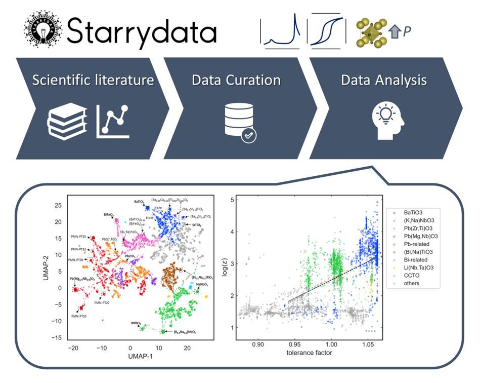
AI-driven materials discovery has great potential to accelerate innovation, but it relies on large and diverse datasets. The lack of such data remains a major bottleneck in the field. To address this challenge, researchers used the Starrydata2 web system to collect experimental data on over 20,000 material samples from more than 5,000 publications. The NIMS team has developed a standardized approach to extract data from graphs, including temperature-dependent properties, which are often omitted in other databases. "What makes our work unique is the meticulous process of manually tracing graphs and correcting inconsistencies in original research papers to create a clean, high-quality dataset," the researchers said.
The database focuses on a specific class of materials necessary for electronics and is the largest ever reported, significantly surpassing previous collections. With this wealth of information, the team used machine learning (ML) to predict the properties of materials and how they would behave electronically.
Although the ML models were effective, they initially worked as "black boxes" — the researchers couldn’t see why the models made their predictions. To understand the context for predictions, the team created visual maps of the data, making complex information easier to interpret. They used clustering algorithms to automatically group similar materials. This analysis helped them spot patterns in how a material's composition affects its properties. The team was also able to categorize the materials into distinct groups, including seven important ferroelectric families, providing a global landscape of the entire compositional space.
The team took a closer look at ABO3 Perovskites, a family of materials which are essential components in everyday electronic devices and energy storage technologies, such as smartphones, computers, and solar cells. Their visualizations showed a simple link between the basic structure of the material and its dielectric permittivity, which coincides with previous academic knowledge.
This work advances our understanding of dielectric materials and moves research beyond traditional trial-and-error approaches. "By curating the largest dataset as ever and combining various machine-learning methods, we succeeded in visualizing the landscape of the entire compositional space in unprecedented detail," the team explained.
The NIMS team plans to make the dataset publicly available next year, allowing scientists worldwide to leverage it for new discoveries. Future work may involve expanding data collection to include manufacturing methods and processing conditions, allowing for more comprehensive predictions that would link production processes to material properties.
"We hope that this foundational work will inspire similar data collection initiatives and new approaches to materials discovery, ultimately leading to smarter materials development pathways that benefit society through improved electronic technologies," the researchers concluded.
Further information
Tomoki Murata
Murata Manufacturing Co., Ltd.
Email: tomoki.murata258@murata.com
Yukari Katsura
National Institute for Materials Science
Email: KATSURA.Yukari@nims.go.jp
Paper: https://doi.org/10.1080/27660400.2025.2485018
About Science and Technology of Advanced Materials: Methods (STAM-M)
STAM Methods is an open access sister journal of Science and Technology of Advanced Materials (STAM), and focuses on emergent methods and tools for improving and/or accelerating materials developments, such as methodology, apparatus, instrumentation, modeling, high-through put data collection, materials/process informatics, databases, and programming. https://www.tandfonline.com/STAM-M
Dr Kazuya Saito
STAM Methods Publishing Director
Email: SAITO.Kazuya@nims.go.jp
Press release distributed by Asia Research News for Science and Technology of Advanced Materials.
]]>Source: Science and Technology of Advanced Materials
Copyright 2025 ACN Newswire . All rights reserved.